
INTERACTIVE PHYSICS LAB
What powers
AI?
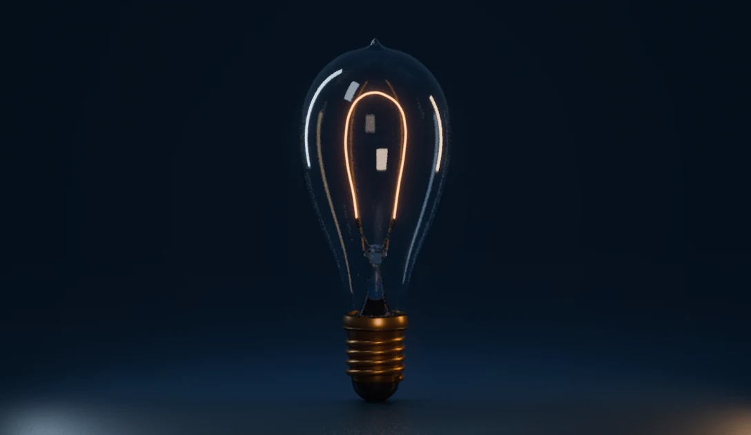
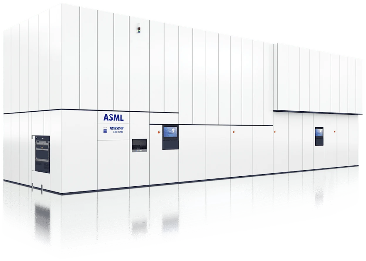
Behind a reply from Jarvis is a chip. Behind the chip is a pattern written with light. Follow the story from Eindhoven’s lamp-making past into ASML’s TWINSCAN EXE:5200B in nearby Veldhoven.
From hot carbon to tin plasma.
From hot carbon to tin plasma.
About 1½ minutes. Pause or take the camera controls at any stop.
The journey
8 stopsOPTICS EXPERIMENT
How fine can light print?
The wavelength stays at 13.5 nm. A larger numerical aperture collects a wider cone of light and resolves finer lines. In a repeating pattern, an 8 nm line beside an 8 nm gap has an 8 nm half-pitch.
Lab notes
Read the eight stops at your own pace.
The scanner
Start beside the two cleanroom engineers. Behind the white panels, this machine exposes the pattern for one circuit layer in a light-sensitive coating on a silicon disk. The tin that makes the light and the wafer that receives it sit in different parts of the machine.
Rotate the enclosure to find the service panels. Lift the cover to see what they hide.
Under the cover
The panels rise away. The modules stay in their working positions. Find the round light-source vessel at one end, the optical assembly closer to the middle and the two wafer tables below it.
Look for the gap between the source and the wafer. What could carry a pattern across it?
Exploded view
The assemblies move apart so you can see how they fit together. One makes light, another gives that light a pattern, and the stage holds the wafer where the pattern comes into focus.
Select a numbered module to investigate it, or follow the tour into the tin source.
Tin to light
A nozzle releases molten tin. Three laser pulses meet each drop. The first flattens it into a sheet. The second spreads the tin into a more diffuse target. The main pulse heats it into plasma, a gas of ions and free electrons. The ions emit light around 13.5 nm.
Scrub slowly to catch the thin sheet before the second pulse spreads it. The curved collector gathers some of the emitted light and sends it toward the optics.
Mirror optics
Air and glass absorb extreme ultraviolet light. Inside a vacuum, three illumination mirrors spread EUV over a reflective master pattern called a reticle and control the angle at which it arrives. At the edges of the pattern, reflected light spreads in several directions. The projection mirrors collect waves that overlap to form the layer’s image.
In this published six-mirror design, follow one representative ray to the wafer. Together they shrink the mask image 4× across the scan and 8× along it. The mask artwork compensates for that difference.
Wafer stage
The silicon disk wears a light-sensitive coating called resist. The wafer and reticle move in step as a slit of patterned light scans one field. The stage positions the next field, and exposure starts again. What leaves the scanner is a wafer with an invisible chemical image in its coating.
Follow the moving slit. A second wafer table allows another disk to be measured during exposure.
From wafer to chip
After a bake, developer dissolves exposed regions of this positive-tone resist. An etcher removes film through the openings. Repeated deposition and patterning build transistors and the wires that connect them.
Follow the change in scale. The fab tests the circuits, cuts the wafer into individual chips called dies, and packages working dies with connections for power, signals and memory.
Inside Jarvis
Imagine one of those dies in the accelerator behind Jarvis. Your prompt becomes small pieces called tokens. The chip works on their numerical values using weights learned during training. The resulting scores help the software choose the next token in a reply.
Follow the glow under the crown. The chip in Jarvis’s head represents the computing behind his voice. His actual chip supply chain is unknown.
Sources & model
In Eindhoven, Gerard and Frederik Philips founded a lamp company in 1891. In 1984, Philips and ASM International formed ASM Lithography in the same city. The team moved to Veldhoven in 1985. The opening lamp is an illustration of early carbon-filament lighting.
Exterior reference image and wordmark by ASML. The cover removal and exploded view are teaching animations based on public module diagrams. The optical close-up traces one representative ray. Its spacing, surface curvatures and folds illustrate the optical sequence. ASML’s installed mirror prescription is proprietary. Colours and process speeds are adjusted for visibility.
- PHILIPSEindhoven and the first lamp factory ↗
- ASMLFrom the joint venture in Eindhoven to Veldhoven ↗
- ASMLEXE:5200B specifications and exterior image ↗
- ASMLFirst full-spec system delivery ↗
- ASMLScanner modules · diagram on page 7 ↗
- EUVLThree laser pulses in the EXE:5200B source · slide 31 ↗
- ASMLSource design and performance · investor presentation ↗
- ASMLLight sources and laser pulses ↗
- ZEISSHigh NA projection optics ↗
- ZEISSScan direction and anamorphic imaging · slide 12 ↗
- SPIEHigh NA optical design · figures 2, 5 and 6 ↗
- ZEISSSix-mirror projection example · figure 1 ↗
- ASMLWafer stages and mechatronics ↗
- ASMLChip manufacturing steps ↗
- TSMCChip-on-wafer-on-substrate packaging ↗
- NVIDIAHow AI inference works ↗